
[use of atmega8/128 with vm as a possibility]
for FPGA, links:
http://setdsp.com/root/products/instrumental/automoduls/setminis2/
http://www.burched.com/ // both for products
a further set of links for CPU design:
http://members.optushome.com.au/jekent/FPGA.htm
In theory:
1] export XILINX=~/Xilinx // where we have our Xilinx distribution
2] ~/Xilinx/bin/lin/promgen -u 0 ~/piksel/fpga_src/tutorail2/tutorial.bit -p exo -s 2048 // make EXO file from our VGA project bitfile
3] xsload -b xsa-50 -flash ~/piksel/fpga_src/tutorail2/tutorial.exo // downloads to the board
to test the last step:...
TESTED on T20 (though strangely xstest fails)
[ see further: http://www.xess.com/manuals/xstools-v4_0.pdf ]
http://www.cs.utexas.edu/users/moore/acl2/v3-0/distrib/acl2-sources/books/workshops/1999/vhdl/
quote:
This directory contains the supporting files for Chapter 11, "Using Macros to Mimic VHDL", by Dominique Borrione, Philippe Georgelin, and Vanderlei Rodrigues, in "Computer-Aided Reasoning: ACL2 Case Studies", edited by M. Kaufmann, P. Manolios, J Moore (Kluwer, 2000, p.167-182).
and:
File fact.lisp is the example in Figure 1. It is the description of the circuit that computes the factorial function, using two concurrent processes. It uses the macros defined in the preceding file.
XSTEND and own FPGA expansion board pin details:
own interface:
8 IN 8 OUT (IN into voltage divider and both by way of 74hc245 transceiver
TOP (4 pin VGA interface)
1: GND
2: 5V
3: VSYNC
4: HSYNC
FPGA XSTEND: ref to FPGA pins (xsa-200/xsa-3s1000):
VERTICAL LINE FROM TOP:
0-7: IN
0: A5/F15
1: F14/P12
2: P9/J1
3: R9/H1
4: T9/H3
5: T7/G2
6: B9/K15
7: A9/K16
0-7: OUT
0: M7/E2
1: R6/E1
2: N7/F3
3: P7/F2
4: R7/G4
5: T14/G3
6: P8/G1
7: T8/H4
(both above as bi-directional I/O ports - extra 16 IN should be available)
0-7: MISC
1: GND
2: 5V
3: VSYNC
4: HYSNC
our components and architecture: Alice in Wonderland, the framed NAND, a mushroom (cloud) spacing, the grid with bottom right hand corner mark shifted up and right, seasonal software and CPU, also morning, afternoon, evening and night sections accessible, Salo circles of hell, Bruegel proverb fragment, quotation,
circular memory and Atrocity exhibition instruction set.
off with her head instruction
from below also:
a) Large Glass - Duchamp. A mechanism (in space).
b) The boudoir/bedroom. A singular eye.
c) Simulated world (billiard ball universe). Kopf. Mushroom cloud neurons.
d) Doubling/ghosting of gates - twinned Alice CPU (also theatre and its double CPU)
but all inputs must be tied down (by connection to FPGA)
http://www.stanford.edu/class/ee183/verilog/183lib.v
To construct components from HDL description in Xilinx WebPAck ISE:
Design utilities -> create schematic symbol
the high- low- level overlap we are interested in
in terms of a methodology of description (code, the diagram, a description of behaviour, software generation of HDL)
after: Design of LISP-Based processors ... or, LAMBDA The Ultimate Opcode
Guy Steele and Gerald Sussman
(http://repository.readscheme.org/ftp/papers/ai-lab-pubs/AIM-514.pdf ) 1979, MIT
see:
1] Architecture reflectes language structure
2] The overlap of high level and machine language is also dictated by necessity to manipulate program as data
3] Programs are represented as nested Lisp data structures -> as a tree of linked records subject to a recursive tree walk
4] Lists are represented by records each of which contains 2 pointers to other records - car and cdr
5] The type field associated with each pointer is used to encode opcodes and return addresses
6] p17 implementation:
7] Two consecutive words of memory hold a list cell - each word can hold a type field and an address field (an address referenced within linear memory)
8] The evaluator and the storage manager as individual processors each with a state machine controller and a set of registers
contents of any register is address field and type field
9] p32 evaluation and procedure call (type 6):
We have a 3-bit type field which provides 8 opcodes (recall 7 as quotation) - address part of a word has different function depending on type (6 is procedure call).
quote:
The evaluation of type 4 (procedure) results in a pointer to the newly allocated word pair. This pointer has type 3 (closure). The car of the pair contains the cdr of the procedure: this is the code body of the procedure. The cdr of the pair contains the current environment.
and:
A procedure call (type 6) is the most complicated... It is a list of indefinite length, chained together by cdr pointers. Each cdr pointer except the last MUST have type 0 (list). The last cdr pointer should have a zero address and a non-ZERO type. This last type specifies the operation to be performed. In CDRing down the list, SIMPLE evaluates each of the expressions in the car, saving the resulting values. These values are available as arguments to the operation to be performed.
operations in tyoe here such as car, cdr, cons, atom, progn, list and funcall
10] further question of recursion in hardware by way of closures:
A closure combines the code of a function with a special lexical environment bound to that function (scope).
5v (TTL a la 74xxxx) to 3.3v (FPGA)
The second thing to do is to insert resistors between the output signals of your 5V circuitry and the gluion's 3.3V inputs. 1k Ohm will do. Furthermore you will need a clamping diode with the anode at your input pin, the cathode tied to 3.3V.
also for matrix 8x8 (chess computer interface):
Some details on the above schematic for the curious: the basic principle of a switch matrix is time-division multiplexing. This is denoted by the pulse diagrams to the left side of the SMR pins where you can see that first SMR0 is pulled low while all other SMR lines are kept high. The system then checks at which SMC pins the pulse arrives, i.e. it now knows which buttons of row 0 are held down. The process is then repeated for each row before re-starting the cycle. This is done at such a high frequency that even the shortest button closure is registered.
The resistors above the SMC pins are internal to the FPGA, i.e. you don't have to supply them yourself. They were implemented to keep the inputs from floating. As a consequence the Switch Matrix is operating in negated mode, i.e. diodes being "reversed" and pulses going down instead of up. However, this should be of no concern to the user, as long as you connect the diodes as shown above.
see: http://www.glui.de/prod/gluion/manual/gManMain.html
.#xxxxx sync and VGA fine 20:05 (2006.10.03:2 tech_notes#283 research#89)
using FPGA for H and V sync
(for RGB from Schmitt triggers remember to link GND from board(s) to box)
~/piksel/fpga_src/tutorail2/
latest .bit as tutorial.bit
FPGA Pins:
Hsync: 85 out
Vsync: 86 out
Input: Output: all bi-directional
0: 67 12
1: 39 13
2: 44 19
3: 46 20
4: 49 21
5: 57 22
6: 60 23
7: 62 26
1] Do we use Schmitt triggers on I/O to provide logic levels (and then limit these with series resistor or voltage divider)?
2] or just use voltage divider in concert with 100 Ohm current limiter
3] or present both options on an expansion board
Test this for VGA throughput!
Its expansion into an 8 bit register (8 simultaneously clocked flip-flops)
or, a 4-bit shift register (data is passed along the chain)
or, a 4 bit counter
1] Can we directly wire analogue signal across the FPGA (say from I/O pin to VGA resistors/input)?:
Using wires and assign. To test.
2] Limiting and/or isolation. All voltages < 3.3v
3] 8 bit to 8 bit - 8 cells or 8x8 matrix of cells. life, cellular automata - that matrix.
Replicated cells composed of micro-structures below:
4] Structures and/or instructions for the CPU:
a) Large Glass - Duchamp. A mechanism (in space).
b) The boudoir/bedroom. A singular eye.
c) Simulated world (billiard ball universe). Kopf. Mushroom cloud neurons.
d) Doubling/ghosting of gates - twinned Alice CPU
e) Further: a passage, quotation, representation. observer embedded
5] Gate diagrams (NOT, AND, NAND, OR, NOR) as artefacts:


6] Gate as switch. see diagrams for transistor multiplex switch symbol in a circle.
Switching across our non-optimal models.
Elaboration of physical circuits (for playing) alongside FPGA - headers and pin extension, break out. Coincident also with software (Lisp) simulation. Machine describing itself, its own coincident layers of active voltage. Reference SICP:
A Simulator for Digital Circuits:
http://mitpress.mit.edu/sicp/full-text/sicp/book/node64.html
and streams: http://mitpress.mit.edu/sicp/full-text/sicp/book/node72.html

7] S/R set-reset flip-flop:
for HDL see: http://myhdl.jandecaluwe.com/doku.php/cookbook:ff

D. flip-flop:
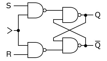
Both based on the NAND gate - a principle of exclusion of the twin (the equivalent/identical binary pair - two ones). Thus of difference enabling a memory. Memory in an active circuit dependent always on current flow. In D flip-flop the clock line straddles the doubled NAND, with a replication of the signal enabling the difference.
Two snakes bite each others tails.
http://www.geocities.com/:/2072/cpudes.htm
and
http://www.geocities.com/:/2072/verilog.htm
see also:
http://www.mindspring.com/~tcoonan/risc8doc.html
http://www.mindspring.com/~tcoonan/pic.v
Using code from:
http://www.stanford.edu/class/ee183/handouts.shtml
we can do very simple sync and when asserted (when we can write as is visible) we can write 6 bits of piksel data (RGB 2 bits for each). next step generate video or connect prototype board pins direct to VGA (thru FPGA? as it has its own 33ohm series resistors or we just send sync out to proto pins and hardwire VGA)
concurrent exposed communicative (promiscuous) (instruction?) modules
exposed by way of PWM or rather single bits which can then be output as audio or as video / composite (with sync generation in software - we have an NTSC example but colour PAL is more complex - also using small resistor ladder to output) or VGA (we have vgahdl example code which looks quite simple)
multiplexed internals, and only internals data access. shared or no registers - how to specify such a design...
Visually:
1] That we can draw components and connect them within a schematic entry which ranges across low and high level (black-boxed) components both from a common library and generated from our own code (using the Create Schematic Symbol entry under Design Utilities in Process).
We can access such created components under the filepath in Categories in the schematic editor when we create say a new overarching design which specifies the connection of large-scale modules/components.
2] That we can (when we select new source) choose further modules from the IP (Coregen & Architecture Wizard) option - this are classified as to various categories, including DSP, math functions, memories, and basic elements such as counters and multiplexors.
3] At the same time using the View/Edit Placed Design (Floorplanner) (under Processes: Implement, Place and Route) we can see how the logic circuitry and I/O are assigned to the CLBs (configurable logic blocks).
From the Floorplanner toolbar we can toggle ratsnest (connection) display and zoom in and out.
Macro and micro views:


http://www.frank-buss.de/lispcpu/index.html
which defines in Verilog output (pins) RAM (on the FPGA), program counter, registers and very basic evaluator (which evaluates hard-coded instructions) - the output in this instance is to slowly flash one LED! This example demonstrates I/O pin assignment
further SDRAM:
http://www.xess.com/appnotes/an-071205-xsasdramcntl.html
Describes/implements/wraps up an SDRAM controller core.
audio:
In the instance of audio perhaps rather than dealing with the on-board audio codec of the XSTend borad, perhaps we should make use of raw 8 bit I/O from prototype area (to primitive soundcard or schmitt trigger box) - prototype area can be connected to adjacent J4 which accesses all the prototype pins from the XSA-50 header (we can look this up in the manual for assignment).
and video:
We can use VGA (some cores/sample projects - note that a useful experiment would be to send voltages (0->0.7v) for RGB signals raw to monitor... or we can use video out on XSTend board, or just resistor ladder from XSA-50 data pins as suggested in ntsc example on:
http://www.xess.com/ho03000.html
where we find all project examples.
Boards used:
XSA-50 development board (Xilinx XC2S50 FPGA (Spartan II/2), 128K Flash memory for FPGA bitstream, 8 Megabyte DRAM).
and XSTend board V3.0 (XST-3.0) from XESS
(stereo codec, dual channel analogue I/O, video decoder, ethernet, usb, rs-232, ide)
see:
http://stewks.ece.stevens-tech.edu/CpE487-S05/HomeworkF04/:/hlisiteB/NotesForXessBoard.html
... example code is in VHDL.
see also free_fpga_guide for some background and install of Xstools from XESS:
link: Xstools RPM: http://www1.cs.columbia.edu/~sedwards/software/xstools-4.0.3-1.i386.rpm
x____
stages:
0] Re-install WebPack (this version 8.2.02i) from Xilinx:
http://www.xilinx.com/webpack/
1) using web-based installer which is a very lengthy process.
2) then we use the opening lines from the shell script at:
http://panteltje.com/panteltje/fpga/index.html
(which outlines solely commandline use of Xilinx toolset.)
mkdir /usr/local/lib/xilinx/
cp ~/Xilinx/bin/lin/*.so /usr/local/lib/xilinx/
echo /usr/local/lib/xilinx >> /etc/ld.so.conf
ldconfig

and:

export XILINX=/root/Xilinx
then we can run bin/lin/xst commandline program
for full GUI:
bin/lin/ise
1] connect parallel port. start laptop. power up XSA-50 board. launch xstest from commandline to test:
xstest -b xsa-50
launch WebPack (command: Xilinx/bin/lin/ise)
2] create new project (here we define the device and the design flow)
Over the above tutorial and past work there is now a new project wizard - we skip over behaviourals and ports:

we create leddec (LED decoder as per tutorial)
3] insert VHDL module (describe/enter (in) VHDL code)
Double click on leddec in sources and edit templated source code.
4] synthesize - highlight module filename .vhd
Click on Synthesize-XST in Processes. Successful
5] implement design process eg. place and route
Highlight and then select Implement Design in Processes
6] new source - implementation constraints (I/O pins assigned as below). then Create Timing Constraints, then port tag:
Select leddec in Sources, right click and select New source following the example names as leddec_ucf, associate this with leddec and then expand User Constraints item in processes to access Create Timing Constraints - once there (new window opened for constraints editor) we can select the Ports tab to access port name attributed in our VHDL and hopefully assign pins (location) as gathered from XESS manual.
In this instance unable to enter text into Location field...
Rather we must choose Assign Package Pins from User Constraints in Process and enter pins here - then these can be double-checked in the above editor.

7] rerun implement design
Successful!
8] generate bitstream - Generate Programming File
Successful!
9] use xsload to download over parallel port - .bit file (in our project file as defined:
xsload -b xsa-50 -fpga ~/piksel/fpgatests/leddec/leddec.bit

Configure FPGA:
Downloading leddec.bit:fst field: ignoring 9 bytes
100%
(strangely enough produces an error when run from eshell)
in the first example LED decoder from the above URL the xsport utility is used to send bit patterns to the parallel port:
eg:
xsport 101
b) understanding of RAM and I/O pin access with XTEND board - again using example code. also perhaps audio and simple video
I/O pin access (which is used within Implementation Constraints (ucf file)) is simply a matter of looking up pin assignments in the manual. The example above also gives some advice.