-->
ap/xxxxx
__
Loosely following excellent tutorial at:
http://www.kicadlib.org/Fichiers/:_Tutorial.pdf
as referenced from:
http://www.kicadlib.org/
- step one: use of EESchema to construct/edit schematic is simple
enough. remember to annotate schematic - use schematic annotation icon
in top bar and select annotate - this gives all components unique
identifiers. then use generate netlist icon and save netlist
- step two: next up schematic modules have to be associated with
physical representation/footprints - run Cvpcb from icons. we have a
list of parts and we need to associate these with scrolling left hand
list of footprints (double click on appropriate footproint when we
have component selected). save this new netlist
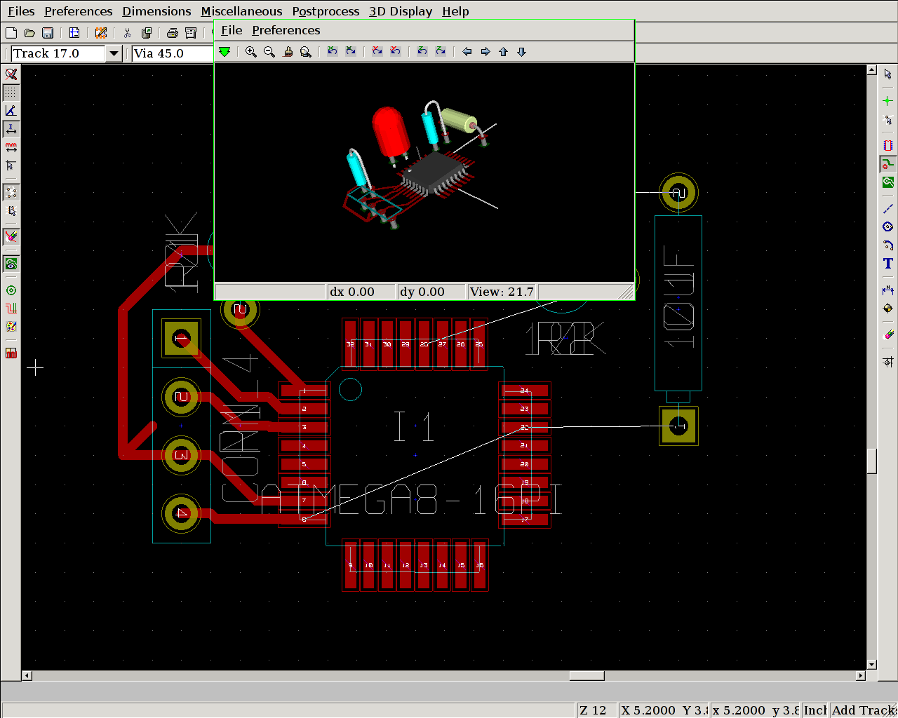
- step three: we run Pcbnew from icons. we need to set paper size from
icon and dimensions of tracks and the like from top menu item. Click
read netlist button, select approrpiate list and hit read. options for
ratnesting are specified in the tutorial - move modules into centre of
sheet and manipulate (move, rotate) until number of crossing points is
reduced. autoroute functionality appears missing as we do not have the
anneal code (?). route by hand using right add tracks icon. for smd we
are working on component level. to print use accurate scale 1 option.
[question remains of how to adapt drawing for mandalas offering up
GND, 5V, TX, RD serial circling the central processor - perhaps making
use of graphic drawing (only of use on silkscreen layers) and print
these at same time]