
http://1010.co.uk/cywm6935.lib
[For physical module in pcbnew used 2x6M header from Eagle libraries and changed first pad.]
1] For both the battery power management and USb interface boards the tantalum SMDs were two small on the PCB. Within pcbnew can replace old part with the right sized (chosen now as C package - 6032) package by selecting [edit module] followed by [change module]. All the different surface mount packages (SMD) were found in:
http://library.oshec.org/library/rc-master.mod
which we load by hand for the project.
2] With the new part inserted connections are lost (eg. netlist, rat's nest). To remedy this, right click on appropriate pad and select [edit pad] option and change pad-net-name to appropriate net (eg. GND, N-00004)
3] To fix our custom, Eagle-imported module [CR2450_KEYSTONE battery halter/holder from Farnell] so that pads are on component surface edited the module file itself (_custom.mod) and changed:
At SMD N 00000000
to:
At SMD N 00888000
1] Plot -> PDF route sometimes chops board - simply reposition on grid
2] Remember to mark tracks/pads which should be attached to the (GROUND) fill before filling the zone
In PCBNEW:
PgUp and PgDn or Shift V to switch component/copper side when laying tracks and vias (to place via start on component side, drag track, right click to place via and then track continues on copper side)
F1 zoom in
F2 zoom out
F3 redraw (across also all kicad apps)
F4 centre at cursor
and further see also: http://xtronics.com/reference/kicad.html
TODO: check SMD sizes and quartz surface mount footprint
http://1010.co.uk/images/scrymain.pdf
Notes:
1] All power/conditioning is done on power module board (but thinking about it maybe put some capacitors across Vcc/GND close by - maybe not- TODO) - thus we expose 5v/3.3v input - 8x ADC, 8x digital pins, serial stuff
Notes:
1] Plenty of very useful libraries inc. for ATmega128 and the Hitachi 32Kx8 Static RAM: 62256 (also from Reichelt) at:
The ATmega128 at: http://library.oshec.org/library/avr.lib
62256: http://library.oshec.org/library/memory-hitachi.lib
2] Making and connecting buses:
From Kicad online help:
In fact, due to the repetition command (Insert key), connections can be very quickly made in the following way, if component pins are aligned in increasing order (a common case in practice on components such as memories, microprocessors…):
Place the first label (for example PCA0)
Use the repetition command as much as needed to place members. EESchema will automatically create the next labels (PCA1, PCA2…) vertically aligned, theorycally on the position of the other pins.
Draw the wire under the first label. Then use the repetition command to place the other wires under the labels.
If needed, place the bus entries by the same way (Place the first entry, then use the repetition command).
Which boils down to:
1] When we export by way of plot option and then ps2pdf and then into GIMP the image is too small. We need to scale X and Y in the plot option to 1.08.
2] To test boards with three options:
a) latest foggy transparency paper
b) clear OHP film
c) foggy as diffuser and then with clear OHP film
... for SMT, double-sided, new VLF design, spectral boards (inc. TV transmitter)
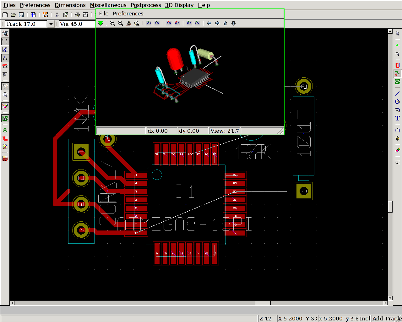
1] In Pcbnew app now we need to fix on trace sizes for non_SMT/D parts:
0.8mm track
0.8mm via drill
0.2mm clearance (or thicker 0.035inch tracks)
We set this in: Top menu: Dimensions. Then Tracks and Vias.
2] Set page-size when we start to A4 under: Top toolbar - page settings icon
3] We needed to add a module which wasn't in the netlist/schematic - it was easy to add using right hand add-module-icon but adding a track wouldn't work - to do this we needed to turn off DRC in Top menu: Preferences and the General Options (or use left hand top icon)
4] We follow tutorial instructions for fill - use right hand zones icon, trace round board size and then right click and fill but it ignores our new tracks (see 3]): (as a compromise we can use the Fill Zone include pads option which leaves the centre free)
[below:
Printing for PCB machen from PCBNEW/KiCad: (2007.01.16:1 tech_notes#10 pcb#2)
1] Straight print from PCBNEW menu under a range of options is unusable (tracks joined, offset and pads connected randomly).
2] Choose plot with Postscript option from file menu and write (in this case) xxxxx-Component.ps. Printing from this using gv is better but unusable also.
3] Run ps2pdf on this .ps and open resulting .pdf with xpdf. Print from this.
(further notes: print command for our CUPS shared printer is lpr -P printer, resolution was set by way of web interface to 600 dpi)
Printing for PCB machen - foto resist using the Gimp: (2007.04.23:2 pcb#5 tech_notes2#3)
1) Import the PDF into the Gimp (open and set resolution to 600). Manipulate and copy as required as a layer.
2) Print settings: Set Image to line and output to Black and White
1] Added library for the older but more manageable FT232BL USB UART (USB to serial) component using online library component builder at:
http://www.rohrbacher.net/kicad/quicklib.php
library is at:
http://1010.co.uk/images/FT232BL.lib
packaging is TQFP32
2] Schematic is at:
http://1010.co.uk/images/atmega8usb.pdf
(note older PCB screenshot is incorrect)
3] 3 projected boards - independent UART and ATmega8 with circles for cpu_model, and both combined as above for 8 bit data interface sans parallel port
Loosely following excellent tutorial at:
http://www.kicadlib.org/Fichiers/:_Tutorial.pdf
as referenced from:
[question remains of how to adapt drawing for mandalas offering up GND, 5V, TX, RD serial circling the central processor - perhaps making use of graphic drawing (only of use on silkscreen layers) and print these at same time]
http://kicad.bokeoa.com/wiki/index.php/Mini_tutorial
to edit a schematic and generate a netlist before we make a PCB design in pcb (all GNU free software) - pcb is installed under Gentoo with seperate emerge command.
http://geda.seul.org/wiki/geda:gschem_ug
and the warmup:
http://www.geda.seul.org/docs/current/tutorials/gsch2pcb/gschem-warmup.html
perhaps try CVS version
Progress so far:
What are the differences here between Default - reference component, embed component and component as individual objects (latter option seperates out and can thus be edited)?
Use reference I think...
ATmega8 component lacks VCC and GND and pin 1 is in an awkward place. First two remedied by modal operation/keystroke driven approach ... where we want pin ap keys and pull line with left mouse into body of chip. middle mouse to stop behaviour. an to add net/wire with similar results. select object with left mouse squaring over and add aa to attach/add attribute such as a pin number. ea to edit attributes of selected piece/element.
er to rotater elements, fs to save, z and Z to zoom, w to zoom next selected square, ve to view extents (?)
But how do we edit the ATmega8 stuff as it stands to switch pin 1?
(only problem is crashes on update)
see Wiki above:
Update Component (ep)
warmup above is a good place to start for simple operations.
note also:
it only makes sense to create pins while creating or editing symbol files...
note also url for gattrib: http://www.brorson.com/gEDA/gattrib/